RTP rapid annealing furnace promotes the development of semiconductor industry
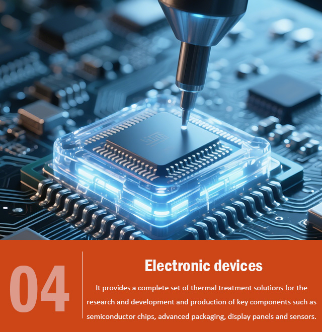
Compound semiconductors have shown great application prospects and development space in cutting-edge technology fields such as new energy, 5G communications, the Internet of Things, and AI artificial intelligence. With the widespread use of third-generation semiconductor materials such as SiC and GaN, driven by application upgrades, the requirements for thermal treatment technology for wafers and compound semiconductors are becoming increasingly higher. The traditional furnace tube annealing process uses long-term high-temperature treatment to eliminate ion implantation damage, stress release, etc., but there are problems such as incomplete defect elimination, long annealing time that easily leads to impurity redistribution, and difficulty in temperature field control. Therefore, a new annealing solution with controllable annealing temperature and higher annealing efficiency is needed.
Principle of RTP Rapid Annealing Furnace
RTP (Rapid Thermal Processing) rapid annealing furnace is a device used for semiconductor device manufacturing and material research. The principle is to change its properties or structure by controlling the temperature and time during heating and cooling, thereby achieving precise control and optimized processing of materials.
Advantages of RTP rapid annealing furnace
The rapid heating process and short duration of RTP rapid annealing furnace can repair lattice defects, activate impurities, and optimize the conductivity after ion implantation. It provides more advanced temperature control, which can achieve annealing in seconds, improve annealing efficiency and effectively save production costs.
In order to meet the needs of the rapid development of the market, Zhengzhou Kejia Electric Furnace Co., Ltd. actively explores the application of rapid thermal annealing. With many years of technical advantages and industry experience, it independently develops and launches RTP fully automatic rapid annealing furnace, which is widely used in the production of various chip products such as IC wafers, LED wafers, MEMS, compound semiconductors and power devices, rapid alloying, ion implantation annealing, oxide growth, metal alloys, etc., through rapid heat treatment to improve crystal structure and optoelectronic properties.
Technical advantages of Zhengzhou Kejia Electric Furnace's RTP rapid annealing furnace
1. Using halogen infrared lamps as heat sources and extremely fast heating rates, the process range covers 200-1250℃.
2. Powerful temperature field management system with high overlap of average temperature curves.
3. Unique patented temperature control system to monitor and correct chamber temperature in real time.
Suitable for silicon wafers of various sizes, second-generation and third-generation compound materials, etc., with excellent heat source and structural design. Double-sided halogen lamps are used as heating sources for rapid annealing processes. The lamp power PID temperature control can accurately control the temperature rise and ensure good temperature reproducibility and temperature uniformity. Welcome to consult and purchase.





 E-mail:web@kejiafurnace.com
 Tell:+(86) 18037178440
 Whatapp:+(86) 180-3717-8440
 Address:Room 1505, Building 9, No. 26 Dongqing Street, Zhengzhou High-tech Industrial Development Zone
