Principles and applications of PECVD/LPCVD/CVD equipment
Chemical Vapor Deposition (CVD) is a technology that deposits solid thin films on the surface of a substrate through gas-phase chemical reactions. Depending on the reaction conditions, CVD can be divided into many types, of which **PECVD (plasma enhanced chemical vapor deposition) and LPCVD (low pressure chemical vapor deposition)** are two important variants. The following is a comparison of their principles, characteristics and applications:1. Conventional CVD (chemical vapor deposition)
Principle:
At high temperatures (usually 500~1200°C), gaseous precursors (such as SiH₄, NH₃, WF₆, etc.) react chemically on the surface of the substrate to generate solid thin films (such as SiO₂, Si₃N₄, W, etc.).
The reaction is usually carried out under normal pressure or low pressure.
Features:
High temperature: requires a higher reaction temperature, suitable for high temperature resistant substrates (such as silicon wafers, quartz).
The deposition rate is high, but uneven films may be produced.
The equipment is simple, but the energy consumption is high.
Application:
Semiconductor: Deposition of polysilicon, silicon oxide, silicon nitride films.
Optical coating: Preparation of anti-reflection film, anti-reflection film.
Hard coating: Such as diamond film, silicon carbide coating.2. LPCVD (Low Pressure Chemical Vapor Deposition)
Principle:
CVD reaction is carried out in a **low pressure (0.1~10 Torr)** environment to reduce the collision frequency between gas phase molecules and improve the uniformity of the film.
Usually requires a higher temperature (500~800°C).
Features:
The film has good uniformity and is suitable for large-area deposition (such as silicon wafer batch processing).
Good step coverage, suitable for complex structures (such as deep trench filling).
The deposition rate is low, but the film quality is high.
Application:
Semiconductor manufacturing:
Deposition of **polysilicon (Poly-Si)** for MOSFET gate.
Deposition of **silicon nitride (Si₃N₄)** as a mask or passivation layer.
Preparation of **silicon oxide (SiO₂)** insulating layer.
MEMS (micro-electromechanical systems): such as silicon-based microstructure processing.3. PECVD (plasma-enhanced chemical vapor deposition)
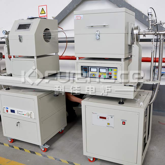
Principle:
Reducing the chemical reaction temperature (usually 200~400°C) with the assistance of **plasma (RF or microwave excitation).
Plasma decomposes the precursor gas, allowing it to be efficiently deposited at low temperatures.
Features:
Low-temperature deposition: suitable for substrates that are not resistant to high temperatures (such as plastics, glass, flexible materials).
Fast deposition rate, but the film may contain more defects (such as high hydrogen content).
Adjustable film stress (such as compressive/tensile stress silicon nitride).
Application:
Semiconductors:
Deposition of **silicon nitride (SiNₓ)** as a passivation layer or anti-reflective coating (ARC).
Preparation of **amorphous silicon (a-Si)** for solar cells or TFTs (thin-film transistors).
Display technology:
Insulating layer or encapsulation layer for OLED and LCD.
Flexible electronics:
Depositing thin films on flexible substrates such as PET and PI.
Optical coating:
Preparing anti-reflection films and anti-scratch coatings.
Comparison summary:
| Parameters |
CVD (normal pressure/thermal CVD) |
LPCVD (low pressure CVD) |
PECVD (plasma CVD) |
| Reaction pressure |
Normal pressure/low pressure |
Low pressure (0.1~10 Torr) |
Low pressure (0.1~5 Torr) |
| Temperature |
500~1200°C |
500~800°C |
200~400°C |
| Deposition rate |
High |
Medium |
High |
| Film quality |
Good |
Excellent (high purity) |
Average (may contain hydrogen) |
| Step coverage |
Average |
Excellent |
Average |
| Main applications |
High temperature film, hard coating |
Semiconductor polysilicon, silicon nitride |
Low temperature film, flexible electronics |
How to choose the right CVD equipment?High-temperature processes (such as SiC, GaN) → Conventional CVD/LPCVD
High uniformity, high-quality films (such as semiconductor devices) → LPCVD
Low-temperature deposition (such as flexible electronics, display panels) → PECVD
Hopefully this comparison will help you understand the applicable scenarios of different CVD technologies! If you need more specific equipment recommendations or process optimization suggestions, please contact us for further discussion.




 E-mail:web@kejiafurnace.com
 Tell:+(86) 18037178440
 Whatapp:+(86) 180-3717-8440
 Address:Room 1505, Building 9, No. 26 Dongqing Street, Zhengzhou High-tech Industrial Development Zone
