CVD vs PECVD Selection Guide: Comprehensive Comparison of Low-Tem Process, Film Quality and Cost
1. Overview of CVD and PECVD Deposition Processes1.1 Core Process Principle and Technical Positioning
CVD relies entirely on high-temperature thermal energy to drive gas-phase chemical reactions, while PECVD uses plasma excitation to replace high-temperature heating, realizing low-temperature thin film deposition.
Chemical Vapor Deposition (CVD) is a traditional thermal-driven thin film preparation process, which decomposes precursor gases and completes film growth on the substrate surface through high-temperature heating. It includes mainstream branches such as APCVD and LPCVD, and is characterized by stable reaction and excellent film crystallinity. Plasma-Enhanced Chemical Vapor Deposition (PECVD) innovatively introduces radio-frequency plasma excitation, which energizes reactive gases at low temperatures to complete chemical cleavage and deposition reactions. The two processes have their own technical advantages, forming a high-temperature high-precision and low-temperature flexible deposition system, which are widely used in semiconductor packaging, MEMS devices, optical coatings and material surface modification fields.
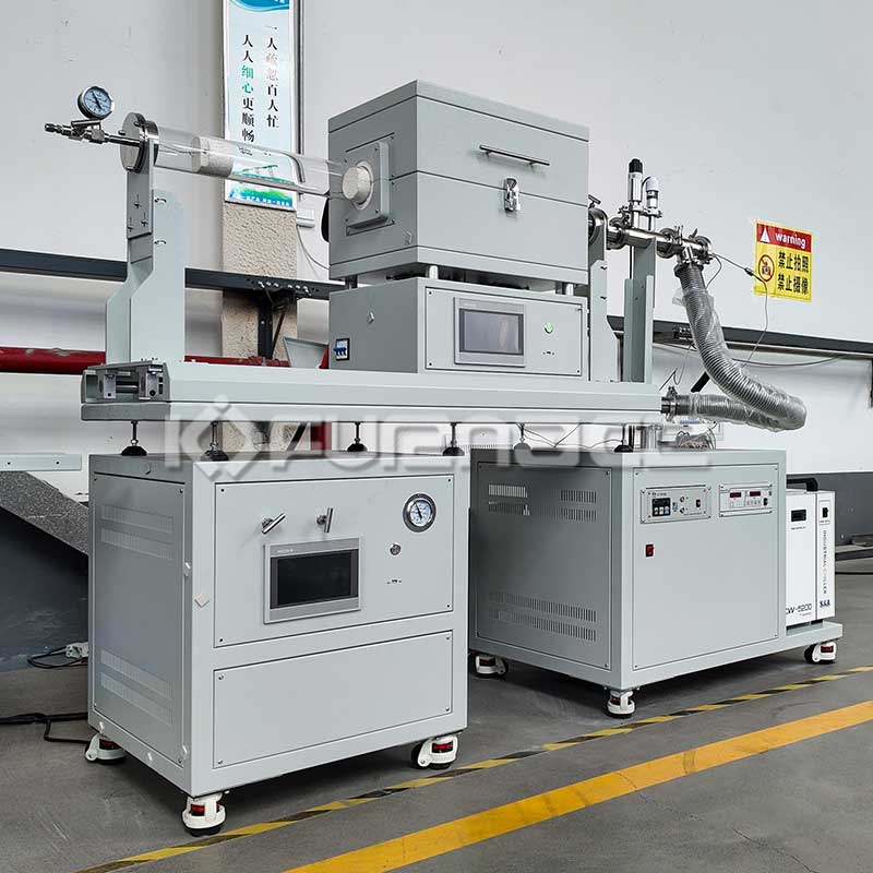
Blind selection of CVD or PECVD leads to thermal damage of heat-sensitive substrates, unqualified film compactness and excessive production costs, restricting process yield and economic benefits.
In actual industrial production, many engineering selections only focus on film formation efficiency and ignore core factors such as process temperature, film stress and operating cost. Using high-temperature CVD for flexible substrates and precision electronic devices will cause substrate deformation, circuit burnout and thermal stress defects; using PECVD for high-crystallinity thin film preparation will lead to insufficient film density and poor high-temperature resistance. The lack of systematic selection criteria based on process scenarios results in inconsistent product quality and uncontrollable comprehensive production cost.
1.3 Comprehensive Comparison and Selection Value
Accurate matching of CVD and PECVD based on low-temperature adaptability, film quality requirements and cost budget is the core of balancing process stability and production economy.
The essential difference between CVD and PECVD lies in the reaction energy source, which derives differences in temperature window, film microstructure, stress characteristics and energy consumption cost. A comprehensive comparison of the three core dimensions of low-temperature process adaptability, film quality performance and full-cycle cost can effectively solve process mismatches, optimize thin film deposition effects, reduce substrate loss and energy waste, and provide standardized technical basis for differentiated process selection in different industrial scenarios.2. Low-Temperature Process Adaptability and Technical Mechanism Comparison2.1 Process Temperature Window and Reaction Characteristics
CVD belongs to high-temperature thermal deposition (450–900℃) with strict substrate temperature tolerance; PECVD realizes low-temperature deposition (150–400℃) with outstanding heat-sensitive material adaptability.
Traditional thermal CVD processes such as LPCVD and APCVD require a high-temperature environment above 450℃ to decompose precursors and drive chemical reactions. High-temperature heating ensures sufficient gas-phase reaction and complete film crystallization, but it is only applicable to high-temperature resistant substrates such as silicon wafers and ceramics. PECVD uses RF electric field to generate plasma, which provides chemical reaction energy instead of heat. It can efficiently complete thin film deposition at 150–400℃, greatly reducing substrate thermal load, and is suitable for heat-sensitive substrates such as polymer materials, flexible films and finished electronic devices.
2.2 Low-Temperature Process Stability and Adaptable Substrates
PECVD has absolute advantages in low-temperature low-stress processing, while CVD cannot replace high-temperature high-crystallinity deposition scenarios due to thermal process characteristics.
In low-temperature working conditions, CVD has insufficient precursor decomposition, slow deposition rate and poor film uniformity, and is prone to pinholes and incomplete film formation. Long-term high-temperature heating will cause thermal warping and performance attenuation of heat-sensitive substrates. PECVD maintains stable reaction efficiency and uniform film-forming effect in the low-temperature range. The low-thermal-balance process avoids substrate thermal damage and residual thermal stress, and can realize low-temperature rapid deposition of SiO₂, SiN and passivation films, which is the mainstream process for flexible electronics and precision device packaging.
2.3 Process Limitations of Low-Temperature and High-Temperature Scenarios
CVD is limited by high-temperature threshold and cannot cover low-temperature flexible processes; PECVD is restricted by plasma mechanism and is not suitable for high-crystallinity thin film preparation.
CVD low-temperature operation will lead to incomplete gas reaction, reduced film density and poor step coverage, failing to meet high-standard passivation and insulation requirements. PECVD plasma bombardment will produce tiny film defects, and the deposited film is mostly amorphous or polycrystalline structure, which cannot achieve the high crystallinity and high thermal stability of thermal CVD films. The two processes have obvious scenario boundaries, and process substitution will directly lead to process failure and product performance degradation.3. Thin Film Quality, Stress and Structural Performance Contrast3.1 Film Density, Uniformity and Step Coverage
CVD films have high density and excellent step coverage, suitable for high-precision structural deposition; PECVD films have uniform flatness and moderate density, suitable for surface passivation and protective coating.
Thermal CVD drives full gas-phase reaction through high temperature, and the deposited thin film has dense microstructure, few internal defects and excellent conformal coverage. It can achieve uniform film growth on complex micro-nano structures and high-aspect-ratio grooves, with outstanding structural adaptability. PECVD plasma uniform ionization ensures flat film surface and good large-area uniformity, but the film density is slightly lower than CVD, and the step coverage capability for ultra-fine complex structures is limited, which is more suitable for flat substrate and conventional structural film formation.
3.2 Film Stress and Structural Stability
PECVD low-temperature film formation effectively reduces thermal stress, while CVD high-temperature film has high structural stability but large residual stress.
CVD high-temperature deposition and cooling cycle are prone to produce large residual thermal stress inside the film, which easily causes film cracking, warping and peeling in subsequent processing, but the film has high hardness, strong wear resistance and excellent high-temperature structural stability. PECVD low-temperature processing has negligible thermal stress, and the film has good flexibility and adhesion, which can adapt to bending and deformation of flexible substrates. However, the film has poor high-temperature resistance, and it is easy to undergo structural relaxation and performance attenuation in high-temperature working environments.
3.3 Electrical and Barrier Properties of Functional Films
CVD films have stable dielectric and barrier properties, suitable for core functional layers; PECVD films have stable insulation and passivation effects, suitable for protective auxiliary layers.
High-density CVD silicon oxide and silicon nitride films have low leakage current, stable dielectric constant and excellent water and oxygen barrier properties, which can be used as core insulation layers and dielectric layers of electronic devices. PECVD deposited films have good insulation and anti-corrosion effects, with low defect rate and stable batch consistency, but the electrical performance is slightly lower than CVD films. They are mostly used for device surface passivation, anti-oxidation protection and surface insulation coating scenarios.4. Full-Cycle Production Cost and Operation Benefit Analysis4.1 Equipment Investment and Site Cost
PECVD equipment has high single investment, simple supporting facilities and low site cost; CVD equipment has low unit price but high supporting thermal system investment and large site occupation.
PECVD integrates plasma power supply, vacuum system and gas path control, with high equipment integration and high single procurement cost. However, it does not need high-temperature heating furnaces and heat insulation facilities, with simple supporting equipment and compact layout, saving plant space cost. Traditional CVD needs to be equipped with high-temperature heating system, heat dissipation device and high-temperature protection structure, with low single equipment cost but high overall supporting investment, large floor area and high early-stage infrastructure construction cost.
4.2 Production Energy Consumption and Operation Cost
PECVD low-temperature operation greatly reduces heating energy consumption, with low long-term operating cost; CVD high-temperature heating leads to high energy consumption and high maintenance cost.
CVD long-term high-temperature operation consumes huge electric energy, and high-temperature components such as heating wires and furnace linings are easy to age and damage, with frequent replacement and high maintenance cost. PECVD relies on plasma energy to drive reactions, the heating system only needs low-temperature auxiliary heating, the overall energy consumption is reduced by 30%–50% compared with CVD, and the loss of high-temperature vulnerable parts is low. Although the plasma system has certain debugging and maintenance costs, the comprehensive energy-saving benefit is prominent in long-cycle mass production.
4.3 Yield Loss and Full-Cycle Comprehensive Benefit
PECVD avoids substrate thermal damage and reduces yield loss; CVD has high film yield but high substrate loss in heat-sensitive scenarios.
In the processing of flexible substrates, precision chips and finished devices, CVD high-temperature process is easy to cause substrate scrapping, with high yield loss and hidden cost. PECVD low-temperature process has no thermal damage risk, stable product yield and low rework rate. In high-temperature resistant substrate processing, CVD has low equipment failure rate and stable film quality, with better comprehensive benefits. The two processes have different cost advantages in different scenarios, and the economic difference is prominent in mass production.5. Scenario-Based Selection Criteria and Industrial Application Prospect5.1 CVD Priority Selection Scenarios
High-temperature resistant substrates, high-crystallinity functional films, high-barrier dielectric layers and high-stability industrial scenarios are exclusive to CVD processes.
For silicon wafer devices, ceramic substrates, high-temperature components and other products that can withstand high-temperature processing, and scenarios requiring high film density, high crystallinity and excellent high-temperature stability such as semiconductor dielectric layers, high-precision barrier films and epitaxial films, CVD thermal deposition process must be selected. It can ensure ultra-stable film electrical performance and structural reliability, and meet the long-term service requirements of high-end electronic devices and precision components.
5.2 PECVD Priority Selection Scenarios
Heat-sensitive substrates, flexible electronic devices, low-stress passivation coating and low-cost mass production scenarios are the core application fields of PECVD.
For flexible films, polymer materials, packaged finished chips and other heat-sensitive substrates, as well as surface passivation, anti-oxidation coating and low-stress film forming processes, PECVD is the optimal choice. Its low-temperature and low-stress characteristics can effectively avoid substrate thermal deformation and performance damage, with fast deposition speed and low comprehensive operating cost, which is very suitable for mass production of consumer electronics, flexible devices and MEMS products.
5.3 Industry Development Trend and Process Iteration Prospect
CVD develops towards high-precision and high-stability functional film deposition; PECVD iterates towards low-temperature ultra-low-stress and intelligent efficient deposition.
With the upgrading of semiconductor miniaturization, flexible electronics and precision coating industries, the process division of labor between CVD and PECVD will be further refined. CVD will focus on high-end core functional layer preparation to meet the demand for high-performance and high-reliability thin films; PECVD will further optimize plasma control and low-temperature process stability, reduce film defects and stress, and expand the application boundary of low-temperature high-quality deposition. The differentiated matching of the two processes will become the mainstream standard for industrial thin film preparation, promoting the high-quality and low-cost development of the thin film processing industry.
Zhengzhou Kejia Technology Co., Ltd. is a high-tech enterprise specializing in R&D and sales of heat treatment products, including muffle furnaces, tube furnaces, vacuum furnaces and more, widely used in metallurgy, ceramic sintering, battery materials, semiconductors, aerospace and other fields.
For inquiries and customized solutions, contact us via WhatsApp: +86 18037178440 or Email: web@kejiafurnace.com.
 English
 简体中文
简体中文 Русский язык
 Français
 日本語
日本語 한국어
한국어 Português
 Español
 Website navigation
 Position:


 Send E-mail:web@kejiafurnace.com
 Wechat/Whatsapp: +86 18037178440
 Company Tell: +(86)18037178440




 E-mail:web@kejiafurnace.com
 Tell:+(86) 18037178440
 Whatapp:+(86) 180-3717-8440
 Address:Room 1505, Building 9, No. 26 Dongqing Street, Zhengzhou High-tech Industrial Development Zone


